Uncovering the Process: What You Need to Know About PCB Manufacturing
- tech4640
- Jul 15, 2024
- 3 min read

In the realm of modern technology, Printed Circuit Boards (PCBs) play a crucial role as the backbone of electronic devices. From smartphones to sophisticated medical equipment, PCBs are the unsung heroes that enable seamless functionality. Have you ever wondered about the intricate process behind the manufacturing of these vital components? Let's delve deeper into the world of PCB manufacturing and uncover the fascinating journey from conception to production.
The Basics of PCBs
Before diving into the manufacturing process, it's essential to understand the fundamental workings of a PCB. A Printed Circuit Board serves as a platform to connect electronic components using conductive tracks, pads, and other features etched from copper sheets laminated onto a non-conductive substrate. These interconnected pathways form the electrical circuits necessary for the device to operate efficiently.
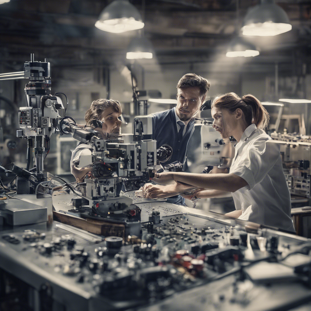
PCB Manufacturing Process
1. Design Phase
The journey of a PCB begins with meticulous planning and design. Engineers utilize specialized software to create a blueprint that outlines the layout of components and the conductive pathways that will be etched onto the board. This design phase is critical, as it sets the foundation for the entire manufacturing process.
2. Material Selection
Once the design is approved, the next step involves selecting the appropriate materials. The substrate material, copper layers, and solder mask are carefully chosen based on the specific requirements of the PCB design. Quality materials are paramount to ensure the reliability and durability of the final product.
3. Etching
The design layout is then transferred onto the copper layers through a process known as etching. A chemical solution or a CNC machine removes the excess copper, leaving behind the desired circuit pattern. Precision and accuracy are key during this step to avoid any defects that could compromise the functionality of the PCB.
4. Drilling
Pinpoint holes are drilled into the board to allow for component placement and electrical connections. Advanced machinery ensures that the holes are accurately positioned according to the design specifications. These holes serve as connection points for the components that will be soldered onto the board later in the process.
5. Component Placement
With the circuit pattern etched and the necessary holes drilled, it's time to populate the board with electronic components. Automated assembly machines carefully place each component onto the board, following the layout specified in the design. This step requires precision to ensure that each component is positioned correctly for optimal functionality.
6. Soldering
The final step in the PCB manufacturing process involves soldering the components onto the board. Solder, a material with a low melting point, is used to create strong electrical connections between the components and the copper traces on the board. This process can be done manually or through automated reflow soldering techniques, depending on the scale of production.
Conclusion
The intricate process of PCB manufacturing combines cutting-edge technology with precision engineering to bring electronic devices to life. From the initial design phase to the final soldering process, every step is crucial in ensuring the functionality and reliability of the end product. Next time you hold a device in your hand, take a moment to appreciate the intricate work that goes into manufacturing the PCB that powers it.
As technology continues to advance at a rapid pace, the world of PCB manufacturing remains at the forefront of innovation, driving the evolution of electronic devices. By understanding the complexity and precision involved in creating these essential components, we gain a newfound appreciation for the intricate world of electronics manufacturing.
Comments